

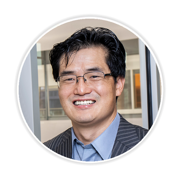
Jeongwon (JP) Park is a professor in the Department of Electrical and Biomedical Engineering at the University of Nevada, Reno. His expertise is in semiconductors, IoT sensors, and sensor networks for advanced manufacturing, nanotechnology-enabled flexible hybrid electronics, nanoelectronics, quantum information science, and nanomaterials.
He is a recipient of the Chinese Academy of Sciences (CAS) President's International Fellowship Initiative (PIFI) at the Beijing Institute of Nanoenergy and Nanosystems (BINN), CAS. He was an associate professor at the School of Electrical Engineering and Computer Science and the University of Ottawa from 2016 to 2019 (currently adjunct professor), and a scientist at SLAC National Accelerator Laboratory, Stanford University from 2014 to 2016. For six years, he served as a senior technologist to support the corporate chief technology officer (CTO) and business units at Applied Materials, USA. He has been a guest researcher at the Lawrence Berkeley National Laboratories, a visiting scholar in the Department of Electrical Engineering at Stanford University, and an adjunct professor in the Department of Electrical Engineering at Santa Clara University.
He received his Ph.D. (2008) in materials science and engineering from the University of California, San Diego, USA. He is a senior member of IEEE and the National Academy of Inventors.
Professor, School of Electrical, Computer and Biomedical Engineering, University of Nevada Reno

Industry Transformation
Q: Having worked in the semiconductor industry for many years, what change over the past decade has surprised you the most?
A: Over the past decade, the most surprising transformation has been how rapidly the semiconductor industry has shifted from being primarily driven by consumer electronics to being fundamentally shaped by artificial intelligence. AI has accelerated demand for high-performance computing, driving innovations not only in leading-edge process nodes but also in chiplet architectures, advanced packaging, 3D chip stacking, and heterogeneous integration. At the same time, geopolitical factors have fundamentally reshaped the global semiconductor landscape through localization efforts, government investments, and supply chain diversification. These changes have made semiconductor innovation as much a strategic and economic priority as a technological one. Looking ahead, I believe the greatest impact will come from advanced packaging and heterogeneous integration, enabling higher performance, lower power consumption, and more cost-effective system designs. As the industry moves toward a multi-trillion-dollar AI-driven economy, success will increasingly depend on combining breakthroughs in materials, manufacturing, system integration, and cross-disciplinary collaboration rather than relying solely on transistor scaling.
Future of Semiconductor Innovation
Q: From your personal perspective, what technological shift in semiconductors do you believe will have the biggest impact over the next decade?
A: From my perspective, the most transformative shift over the next decade will be the convergence of advanced packaging, 3D chip stacking, heterogeneous integration, and artificial intelligence. As traditional transistor scaling approaches its physical and economic limits, future performance gains will increasingly come from integrating diverse technologies—including logic, memory, photonics, sensors, and specialized AI accelerators—into highly efficient systems. This systems-level approach enables significantly higher computing performance, lower power consumption, and faster data movement while reducing development costs through modular chiplet architectures. At the same time, AI will reshape both semiconductor design and manufacturing by accelerating electronic design automation, optimizing fabrication processes, and improving yield through data-driven analytics. Looking further ahead, quantum computing and new materials will complement, rather than replace, conventional CMOS technologies. The future of semiconductor innovation will therefore be defined not by a single breakthrough, but by the integration of multiple technologies working together to address increasingly complex computing challenges.
Emerging Applications
Q: Looking at how technology is evolving, which emerging semiconductor-driven applications do you personally find most exciting today, and why?
A: The emerging semiconductor-driven applications I find most exciting are artificial intelligence, advanced healthcare, and intelligent manufacturing because they have the potential to improve people's lives worldwide. AI-enabled systems are driving breakthroughs in autonomous technologies, scientific discovery, and data-intensive computing, while semiconductor innovations are making these systems faster and more energy efficient. I am also particularly excited about wearable and flexible electronics, IoT sensors, and biomedical devices that enable continuous health monitoring and personalized medicine. In manufacturing, smart sensors and edge AI are transforming factories through predictive maintenance, real-time process optimization, and higher productivity. Looking further ahead, quantum computing and integrated photonics offer tremendous opportunities to solve problems that are beyond the reach of today's computers. What excites me most is that these advances are not isolated innovations—they are enabled by continued progress in semiconductor materials, device architectures, advanced packaging, and heterogeneous integration working together to create entirely new capabilities.
Leadership in a Fast-Moving Industry
Q: From your personal experience, what leadership qualities are most important when working in such a complex and fast-moving technology industry?
A: From my experience, effective leadership in the semiconductor industry requires adaptability, technical rigor, and the ability to bring diverse teams together around a common vision. The pace of technological change, evolving market demands, and global supply chain challenges require leaders to make informed decisions quickly while remaining flexible as conditions change. Equally important is maintaining high standards for quality, data-driven problem-solving, and operational excellence, particularly in research and advanced manufacturing environments where small details can have significant impacts. Strong communication is also essential because semiconductor innovation depends on close collaboration among materials scientists, device engineers, software developers, manufacturing experts, and business leaders. I also believe that great leaders foster curiosity, encourage diverse perspectives, and create an environment where people are empowered to innovate and learn from failure. Ultimately, leadership is about enabling talented individuals to work together effectively to solve complex problems and deliver technologies that create lasting societal impact.
Personal Learning & Curiosity
Q: Technology evolves rapidly—how do you personally stay curious and continue learning in such a dynamic field?
A: Staying curious begins with maintaining the same mindset that first inspired me to take apart a radio as a child—to always ask how things work and how they can be improved. I continuously learn by following the latest developments in semiconductor technology, artificial intelligence, advanced materials, and manufacturing through IEEE, SEMI, leading conferences, and collaboration with researchers and industry partners. Equally important is hands-on exploration, whether experimenting in the laboratory, mentoring students on emerging technologies, or even working on mechanical systems such as automobile repairs. These practical experiences often provide fresh perspectives on solving complex engineering problems. I also believe that learning accelerates by engaging with people from diverse disciplines and backgrounds, since innovation often occurs at the intersection of fields. Remaining open-minded, adaptable, and willing to challenge existing assumptions has been essential to sustaining both my curiosity and my passion for innovation throughout my career.
Advice for the Next Generation
Q: From your perspective, what skills will be most valuable for the next generation entering the semiconductor industry?
A: The next generation of semiconductor professionals will need a strong combination of technical expertise, interdisciplinary thinking, and adaptability. A solid foundation in semiconductor physics, materials science, device engineering, and manufacturing remains essential, but equally important are skills in artificial intelligence, data analytics, hardware-software co-design, and advanced packaging technologies. Hands-on experience in fabrication, characterization, and system integration will help bridge the gap between theory and real-world applications. Beyond technical knowledge, I encourage young engineers to develop strong problem-solving, communication, and teamwork skills, as innovation increasingly depends on collaboration across multiple disciplines and global organizations. Most importantly, cultivate curiosity and commit to lifelong learning. The semiconductor industry evolves rapidly, and those who remain open to new ideas, embrace emerging technologies, and continuously expand their knowledge will be best positioned to drive the next generation of breakthroughs that power future innovations.
Societal Impact and Responsibility
Q: As semiconductor technologies become increasingly powerful, how do you personally think about the responsibility that comes with innovation?
A: As semiconductor technologies become more powerful and pervasive, I believe innovation must be guided by a strong sense of responsibility. Engineers and researchers should consider not only what is technologically possible, but also how their work affects society, the environment, and future generations. This includes developing energy-efficient technologies, reducing the environmental footprint of semiconductor manufacturing, responsibly sourcing materials, and improving the sustainability of fabrication processes. We must also strengthen supply chain resilience and protect the integrity of critical technologies while ensuring that innovation benefits society broadly. As artificial intelligence and advanced computing become increasingly integrated into everyday life, ethical considerations such as security, privacy, and reliability must remain central to technology development. Ultimately, the goal of innovation is not simply to create faster or more powerful devices, but to develop technologies that improve quality of life, advance scientific discovery, and contribute to a more sustainable and equitable future.